kair.us/ projects/ delay_relay/
Delay relay
A simple, solid state delayed off 'relay' for 12V and 24V
systems. You could use it to control a Webasto water pump or CB
radio, or anything you want to be automatically switched off after a
delay.
Circuit operation
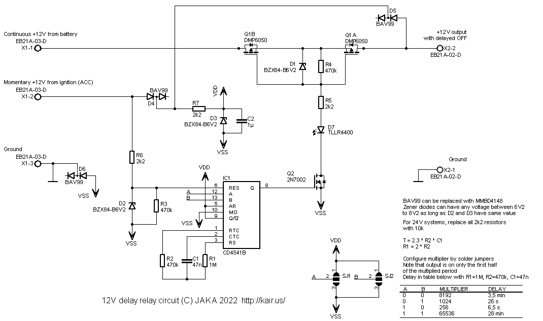
The delay circuit is based on 4541 logic circuit. Despite being an
old chip, it is sill available from several manufacturers, e.g. TI,
NXP and Onsemi. The 4541 contains an oscillator and divider, so it
has everything needed to generate longer delays than a circuit based
on NE555. The schematic diagram is shown below.

The circuit has two inputs. The '12V' is connected to a permanent
+12V supply, such as car battery. The 'ACC' input is connected to a
momentary +12V supply, which acts as control input to delay relay
circuit. The load is connected to screw connector X2. The load is
powered whenever the 'ACC' input is active. The load stays powered
for the delay period and then switches off.
The circuit has many zener and signal diodes. Their purpose is to
protect from all the nasty voltage events that could be encountered
in a vehicle. For example, reverse battery polarity, jump start from
a 24V battery and load dump. They aren't tested to be ISO 7637-2
proof, but the circuit should withstand practical scenarios pretty
well.
The power switch is constructed from two PMOS transistors, which are
integrated into one package. The benefit is reduced power
consumption, size and contact wear elimination. Special attention
has been paid to quiescent current. When the delay has elapsed, the
power from CD4541B IC is completely cut off. So only the leakage
current of the PMOS power switch is draining power, which is
negligible.
You can select from four delay settings, spanning from approx. 7
seconds to almost half an hour. If none of the predefined settings
suit your need, you could tweak C1,R1 and R2 values according to the
equation shown in circuit diagram.
PCB
The PCB is designed with Cadsoft Eagle 5.12.0. It fits Hammond
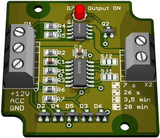
1551RBK enclosure. Below is Eagle 3D rendition of the board.
Input connector is shown on left and output connection at right. The
LED lights whenever the load is powered. You must solder the SJ1 and
SJ2 jumpers according to markings on silkscreen, depending on the
delay length you need.

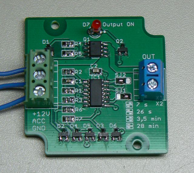
Photo of actual board below. Here I have used mostly 0603 size
passives. They work, but the footprints on board are 0805 size.
Downloads for the design files, Gerber files and documentation are
below. You can order bare boards from PCBWay using this
link. Here is TME
shared project which contains all the components for the
project, except the PCB.
delay_relay_v11.zip
Eagle .sch and .brd
delay_relay_v11.pdf
Circuit diagram, assembly drawing and BOM in PDF format
delay_relay_v11_gerber.zip
Gerber files
kair.us/ projects/ delay_relay/
page created 5.2.2022
last updated 3.10.2022 webmaster@kair.us
